- 您现在的位置:买卖IC网 > Sheet目录3889 > PIC16F1827-I/SS (Microchip Technology)IC PIC MCU FLASH 4K 20-SSOP
190
2570N–AVR–05/11
ATmega325/3250/645/6450
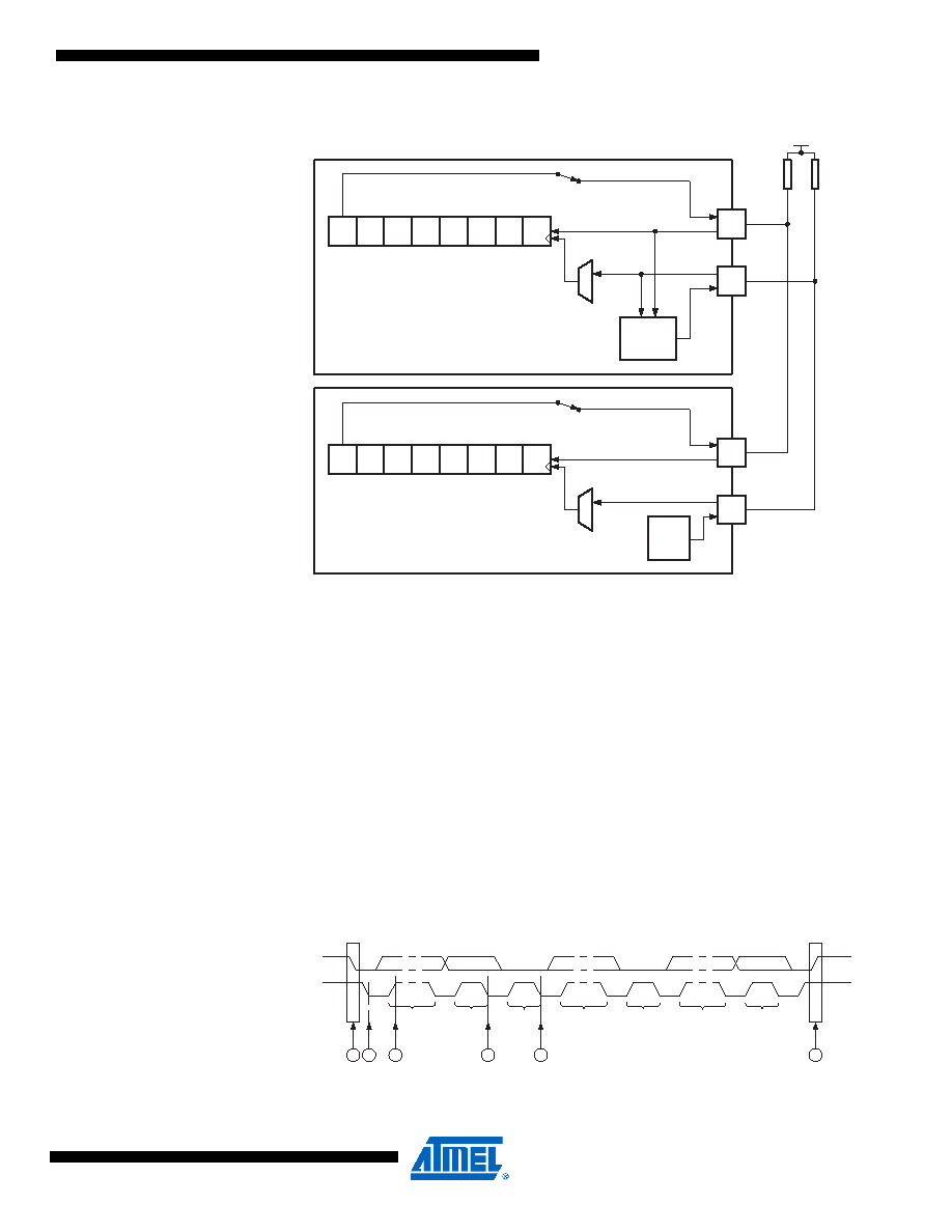
Figure 21-4. Two-wire Mode Operation, Simplified Diagram
Figure 21-4 shows two USI units operating in Two-wire mode, one as Master and one as Slave.
It is only the physical layer that is shown since the system operation is highly dependent of the
communication scheme used. The main differences between the Master and Slave operation at
this level, is the serial clock generation which is always done by the Master, and only the Slave
uses the clock control unit. Clock generation must be implemented in software, but the shift
operation is done automatically by both devices. Note that only clocking on negative edge for
shifting data is of practical use in this mode. The slave can insert wait states at start or end of
transfer by forcing the SCL clock low. This means that the Master must always check if the SCL
line was actually released after it has generated a positive edge.
Since the clock also increments the counter, a counter overflow can be used to indicate that the
transfer is completed. The clock is generated by the master by toggling the USCK pin via the
PORT Register.
The data direction is not given by the physical layer. A protocol, like the one used by the TWI-
bus, must be implemented to control the data flow.
Figure 21-5. Two-wire Mode, Typical Timing Diagram
Referring to the timing diagram (Figure 21-5.), a bus transfer involves the following steps:
MASTER
SLAVE
Bit7
Bit6
Bit5
Bit4
Bit3
Bit2
Bit1
Bit0
SDA
SCL
Bit7
Bit6
Bit5
Bit4
Bit3
Bit2
Bit1
Bit0
Two-wire Clock
Control Unit
HOLD
SCL
PORTxn
SDA
SCL
VCC
P
S
ADDRESS
1 - 7
8
9
R/W
ACK
1 - 8
9
DATA
ACK
1 - 8
9
DATA
SDA
SCL
A B
D
E
C
F
发布紧急采购,3分钟左右您将得到回复。
相关PDF资料
PIC12C508-04/P
IC MCU OTP 512X12 8DIP
22-15-3153
CONN FFC/FPC 15POS .100 RT ANG
PIC16F1826-I/MV
IC PIC MCU FLASH 2K 28-UQFN
PIC16F1825-I/P
MCU PIC 14K FLASH 1K RAM 14DIP
22-02-3153
CONN FFC/FPC VERTICAL 15POS .100
22-15-3143
CONN FFC/FPC 14POS .100 RT ANG
22-02-3143
CONN FFC/FPC VERTICAL 14POS .100
502078-2110
CONN FPC .25MM 21POS R/A SMD
相关代理商/技术参数
PIC16F1827T-I/ML
功能描述:8位微控制器 -MCU 7KB Flash 384 byte 32 MHz Int. Osc RoHS:否 制造商:Silicon Labs 核心:8051 处理器系列:C8051F39x 数据总线宽度:8 bit 最大时钟频率:50 MHz 程序存储器大小:16 KB 数据 RAM 大小:1 KB 片上 ADC:Yes 工作电源电压:1.8 V to 3.6 V 工作温度范围:- 40 C to + 105 C 封装 / 箱体:QFN-20 安装风格:SMD/SMT
PIC16F1827T-I/MQ
功能描述:8位微控制器 -MCU 7KB Flash 384 byte 32 MHz Int. Osc RoHS:否 制造商:Silicon Labs 核心:8051 处理器系列:C8051F39x 数据总线宽度:8 bit 最大时钟频率:50 MHz 程序存储器大小:16 KB 数据 RAM 大小:1 KB 片上 ADC:Yes 工作电源电压:1.8 V to 3.6 V 工作温度范围:- 40 C to + 105 C 封装 / 箱体:QFN-20 安装风格:SMD/SMT
PIC16F1827T-I/MV
功能描述:8位微控制器 -MCU 7KB Flash 384 RAM RoHS:否 制造商:Silicon Labs 核心:8051 处理器系列:C8051F39x 数据总线宽度:8 bit 最大时钟频率:50 MHz 程序存储器大小:16 KB 数据 RAM 大小:1 KB 片上 ADC:Yes 工作电源电压:1.8 V to 3.6 V 工作温度范围:- 40 C to + 105 C 封装 / 箱体:QFN-20 安装风格:SMD/SMT
PIC16F1827T-I/SO
功能描述:8位微控制器 -MCU 7KB Flash 384 byte 32 MHz Int. Osc RoHS:否 制造商:Silicon Labs 核心:8051 处理器系列:C8051F39x 数据总线宽度:8 bit 最大时钟频率:50 MHz 程序存储器大小:16 KB 数据 RAM 大小:1 KB 片上 ADC:Yes 工作电源电压:1.8 V to 3.6 V 工作温度范围:- 40 C to + 105 C 封装 / 箱体:QFN-20 安装风格:SMD/SMT
PIC16F1827T-I/SS
功能描述:8位微控制器 -MCU 7KB Flash 384 byte 32 MHz Int. Osc RoHS:否 制造商:Silicon Labs 核心:8051 处理器系列:C8051F39x 数据总线宽度:8 bit 最大时钟频率:50 MHz 程序存储器大小:16 KB 数据 RAM 大小:1 KB 片上 ADC:Yes 工作电源电压:1.8 V to 3.6 V 工作温度范围:- 40 C to + 105 C 封装 / 箱体:QFN-20 安装风格:SMD/SMT
PIC16F1828-E/ML
功能描述:8位微控制器 -MCU 7 KB Flash 256b RAM 32 MHz Int. Osc RoHS:否 制造商:Silicon Labs 核心:8051 处理器系列:C8051F39x 数据总线宽度:8 bit 最大时钟频率:50 MHz 程序存储器大小:16 KB 数据 RAM 大小:1 KB 片上 ADC:Yes 工作电源电压:1.8 V to 3.6 V 工作温度范围:- 40 C to + 105 C 封装 / 箱体:QFN-20 安装风格:SMD/SMT
PIC16F1828-E/P
功能描述:8位微控制器 -MCU 7 KB Flash 256b RAM 32 MHz Int. Osc RoHS:否 制造商:Silicon Labs 核心:8051 处理器系列:C8051F39x 数据总线宽度:8 bit 最大时钟频率:50 MHz 程序存储器大小:16 KB 数据 RAM 大小:1 KB 片上 ADC:Yes 工作电源电压:1.8 V to 3.6 V 工作温度范围:- 40 C to + 105 C 封装 / 箱体:QFN-20 安装风格:SMD/SMT
PIC16F1828-E/SO
功能描述:8位微控制器 -MCU 7 KB Flash 256b RAM 32 MHz Int. Osc RoHS:否 制造商:Silicon Labs 核心:8051 处理器系列:C8051F39x 数据总线宽度:8 bit 最大时钟频率:50 MHz 程序存储器大小:16 KB 数据 RAM 大小:1 KB 片上 ADC:Yes 工作电源电压:1.8 V to 3.6 V 工作温度范围:- 40 C to + 105 C 封装 / 箱体:QFN-20 安装风格:SMD/SMT